Lead and Lag compensator
Compensators are used to improve the stability and accuracy of a system. It is added to a controller as a plugin to tune the system to meet the system's dynamic performance requirements.
Lead compensator
The lead compensator is an network (typically an RC network) which produces a sinusoidal output having phase lead when a sinusoidal input is applied. It is added to improve the phase margin of a system, which reduces excessive ringing / overshoot in a system. It increases system's bandwidth.

Here, the capacitor is parallel to the resistor R1 and the output is measured across resistor R2. The transfer function of this lead compensator is -
$$\cfrac{V_o(s)}{V_i(s)}=k\left(\cfrac{1+\tau{}s}{1+\alpha{}\tau{}s}\right)$$
Where,
$$\tau{}=R_1C$$ $$\alpha{}=k=\cfrac{R_2}{R_1+R_2}$$
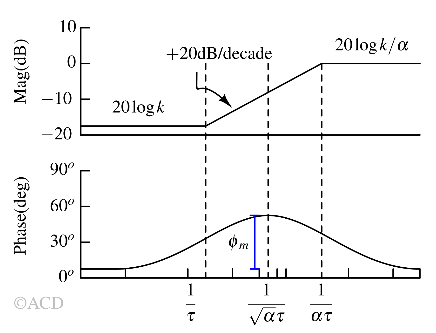
From the transfer function, we can observe that the lead compensator has zero at \(s=1/\tau{}\) and pole at \(s=1/\alpha{}\tau{}\). Since, \(\alpha{}<1\), the zero will appear earlier than the pole in the bode plot.
To find the phase relation, substituting, \(s=j\omega{}\) in the transfer function -
$$\cfrac{V_o(j\omega{})}{V_i(j\omega{})}=k\left(\cfrac{1+j\omega{}\tau{}}{1+j\omega{}\alpha{}\tau{}}\right)$$
Phase angle,
$$\phi{}=\tan^{-1}\left(\omega{}\tau{}\right)-\tan^{-1}\left(\alpha{}\omega{}\tau{}\right)$$
Maximum phase is added at frequency (where \(d\phi{}/d\omega{}=0\)),
$$\cfrac{d\phi{}}{d\omega{}}=\cfrac{\tau{}}{1+\left(\omega{}\tau{}\right)^2}-\cfrac{\alpha{}\tau{}}{1+\left(\omega{}\alpha{}\tau{}\right)^2}=0$$
$$\omega{}_m=\sqrt{\cfrac{1}{\tau{}}\cfrac{1}{\alpha{}\tau{}}}=\cfrac{1}{\tau{}\sqrt{\alpha{}}}$$
The frequency where maximum phase occurs is the geometric mean of pole and zero frequency.
Maximum phase,
$$\phi{}_m=\sin^{-1}\left(\cfrac{1-\alpha{}}{1+\alpha{}}\right)$$
Lag compensator
The lead compensator is an analog circuit network which produces a sinusoidal output having phase lead when a sinusoidal input is applied. It is added to improve the phase margin of a system, which reduces excessive ringing / overshoot in a system.

Here, the capacitor is in series with the resistor R2 and the output is measured across this combination. The transfer function of this lead compensator is -
$$\cfrac{V_o(s)}{V_i(s)}=k\left(\cfrac{1+\tau{}s}{1+\beta{}\tau{}s}\right)$$
Where,
$$\tau{}=R_2C$$
$$\beta{}=\cfrac{R_1+R_2}{R_2}$$
$$k=1$$
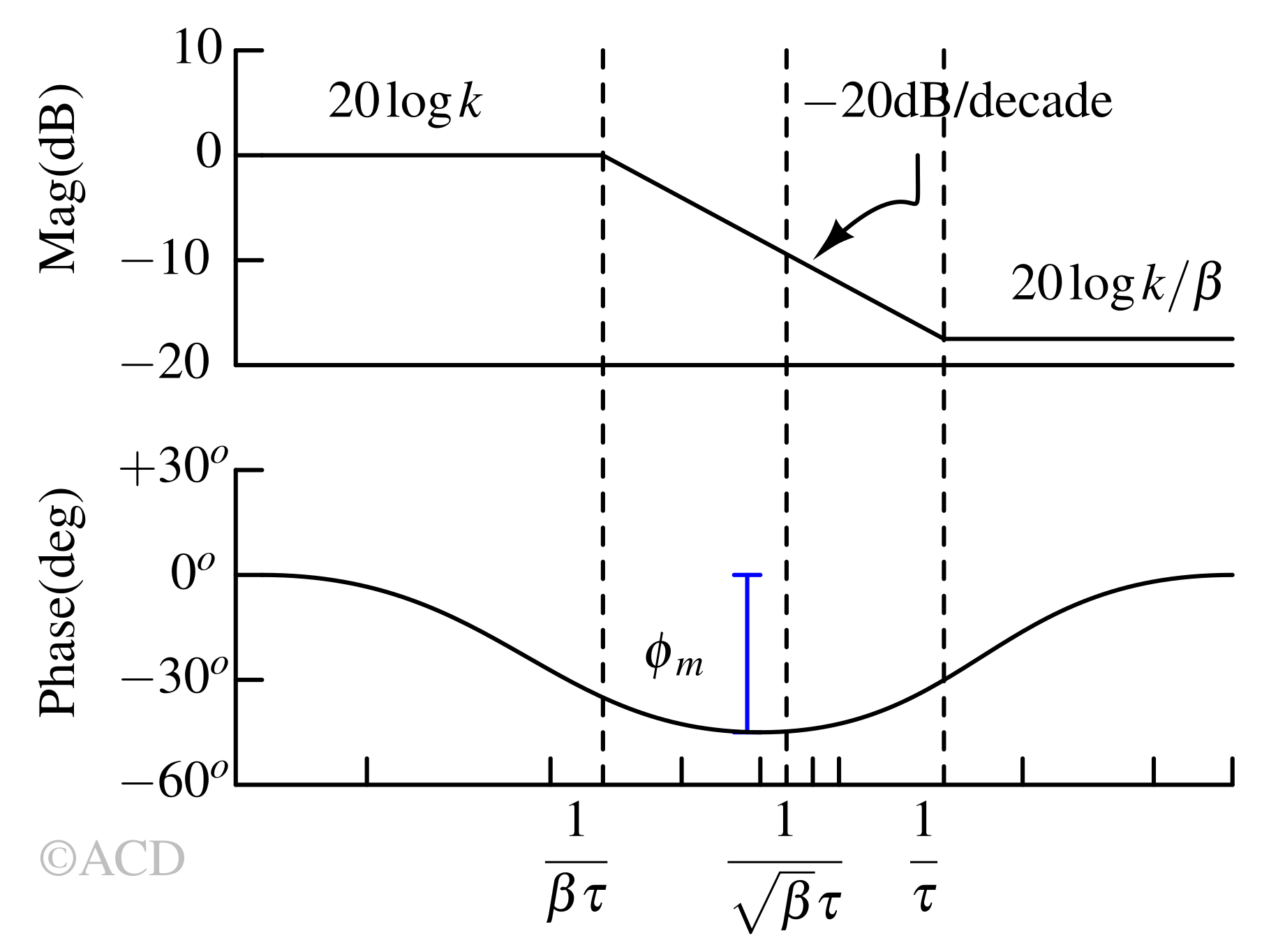
From the transfer function, we can conclude that the lag compensator has one pole at \(s=1/\beta{}\tau{}\) and one zero \(s=1/\tau{}\). Since, \(\beta{}>1\), the pole will appear earlier than zero in the bode plot for the lag compensator.
To find the phase relation, substituting, \(s=j\omega{}\) in the transfer function -
$$\cfrac{V_o(j\omega{})}{V_i(j\omega{})}=k\left(\cfrac{1+j\omega{}\tau{}}{1+j\omega{}\beta{}\tau{}}\right)$$
Phase angle,
$$\phi{}=\tan^{-1}\left(\omega{}\tau{}\right)-\tan^{-1}\left(\beta{}\omega{}\tau{}\right)$$
Maximum phase is subtracted at frequency,
$$\omega{}_m=\sqrt{\cfrac{1}{\tau{}}\cfrac{1}{\beta{}\tau{}}}=\cfrac{1}{\tau{}\sqrt{\beta{}}}$$
The frequency where minimum phase occurs is the geometric mean of pole and zero frequency.
Maximum phase,
$$\phi{}_m=\sin^{-1}\left(\cfrac{\beta{}-1}{\beta{}+1}\right)$$
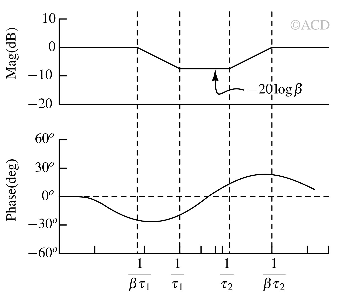
Lead and Lag compensator
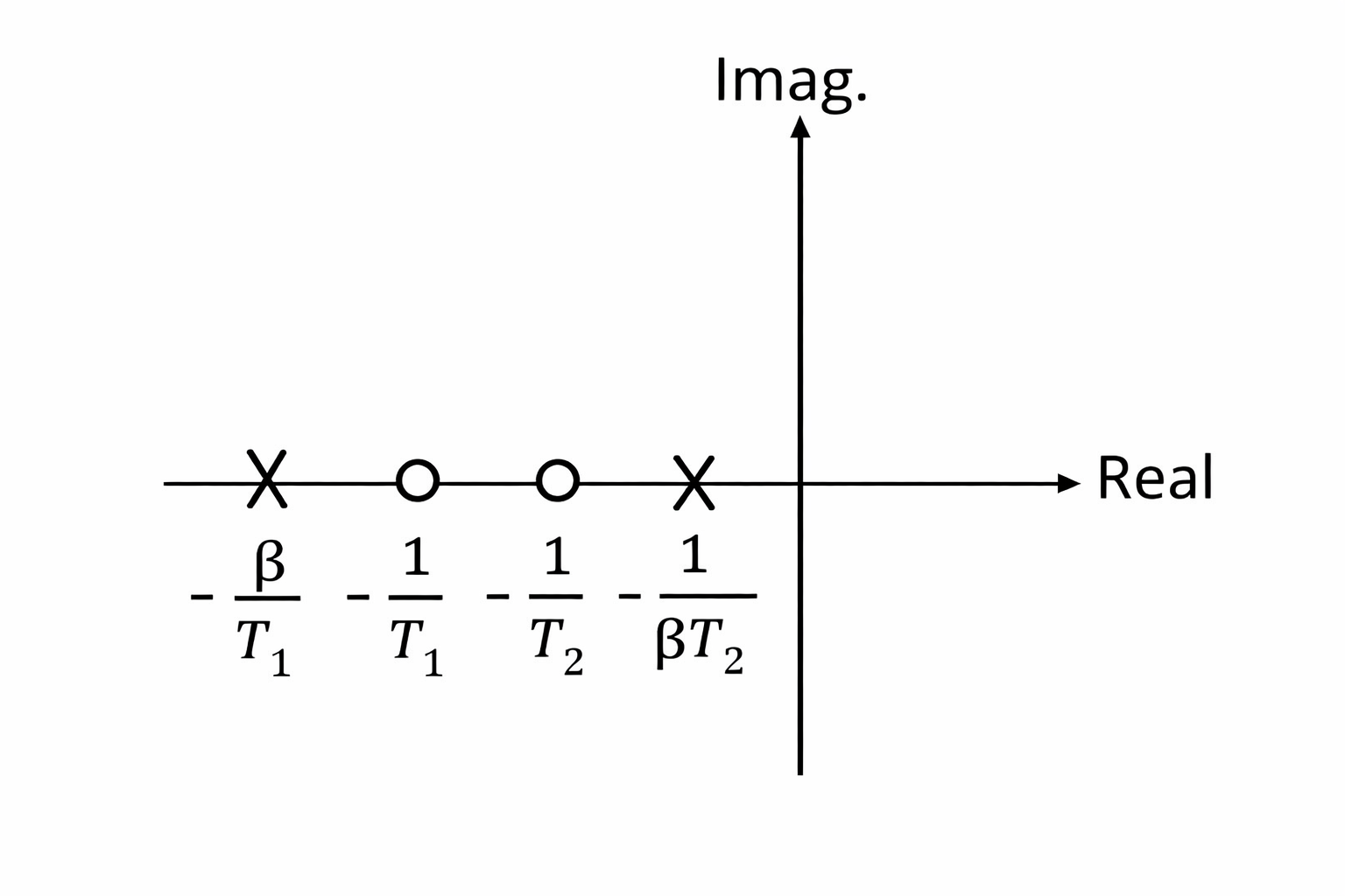
We can also combine the two types of compensators listed above to yield a lead-lag compensator. Sometimes, both effects are needed — faster rise/fall (lag-compensator) and reaching steady-state faster without ringing (lead compensator). This is similar to PID tuning.

Compensator equation :
$$D(s)=\cfrac{\tau{}_1s+1}{\alpha{}\tau{}_1s+1}\cfrac{\tau{}_2s+1}{\beta{}\tau{}_2s+1}$$
Where,
$$\beta{}>1$$ $$\alpha{}<1$$ $$\tau{}_1,\tau{}_2>1$$
To simplify the design equation, we can add a condition \(\alpha{}=1/\beta{}\),
$$D(s)=\cfrac{\tau{}_1s+1}{\beta{}\tau{}_1s+1}\cfrac{\tau{}_2s+1}{\cfrac{1}{\beta{}}\tau{}_2s+1}$$